MUR Blog - How to Manually Create Footprints in Altium Designer
Printed circuit boards (PCB) are essential in almost all commercial devices that contain some form of electrical circuits because of its flexibility and compactness. Custom designed PCBs can achieve the exact function we want while saving all the spaces we can and plus the circuit is more stable on a PCB due to its protective coating. At MUR, we design and manufacture PCBs for low voltage systems, battery management systems, electric power train, accumulator etc. For example, the safety system, voltage monitoring system, cell balancing systems are designed and manufactured onto PCB boards.
When designing PCBs for various purposes, it’s almost impossible to avoid the headache of finding footprints because the manufacturer in most cases only supplies us with a data sheet but no footprint files. A footprint defines the land layout pattern of a component on a PCB (the shiny silver pads in the photo below). The photo below is a prototype PCB of our cell balancing system before the components being soldered on. The ones with holes are for ‘through hole’ type components and the ones without are for surface mount components.
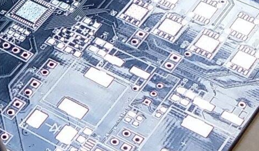
MUR Cell Balancing System PCB
This article will focus on surface mount components; I’ll go through two examples of creating footprints for surface mount components in Altium Designer. In the first example, I will teach you how to use the IPC Compliant Footprint Wizard step by step. Next, I will demonstrate how a completely customized footprint can be created from scratch.
IPC Compliant Footprint Wizard
In this example, we will be creating a footprint for ‘ADuM3151’, a 3.75kV, 7-Channel, SPI Digital Isolator from Analog Devices, this isolator is used in our BMS design to help isolate the High Voltage systems with Low Voltage systems.
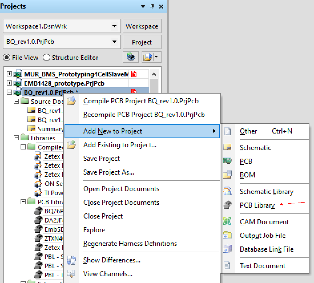
- Create a PCB Library file within the project as shown below.
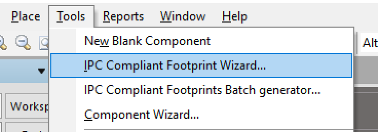
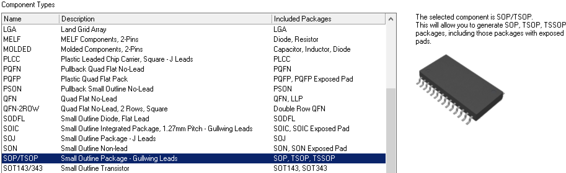
- Click on Tools and you will see the IPC Compliant Footprint Wizard.
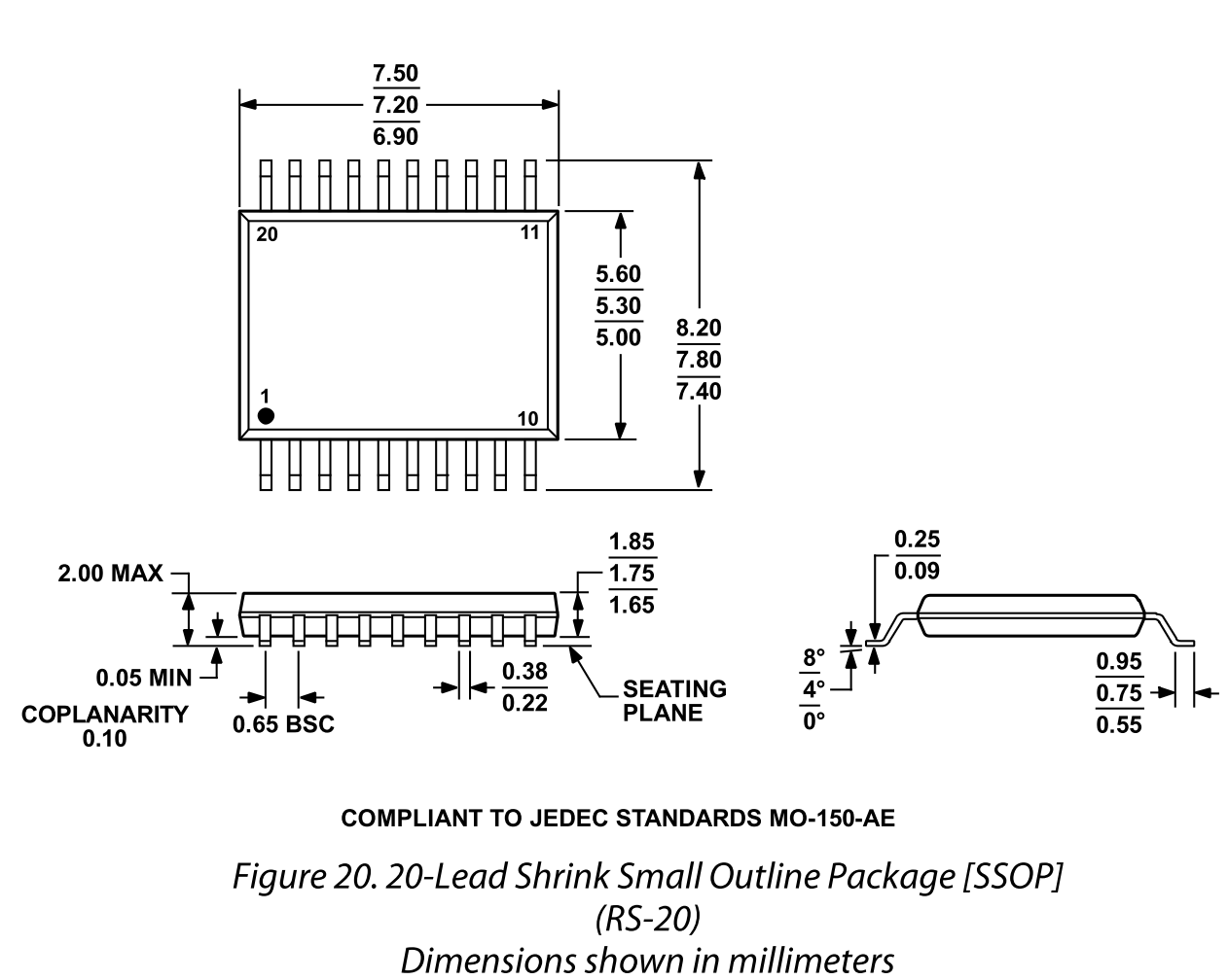
- Find the Outline Dimensions page from the data sheet.
- Select the component type according to the data sheet and component shape.
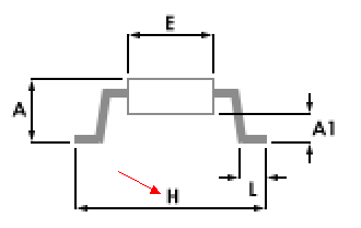
- Enter data according to data sheet. All data entries have a name and a letter in brackets. It’s easier to figure out what the data entry is by finding the corresponding letter in the diagram. For example, the first data entry is ‘Width Range (H)’. In the diagram next to it, we see what H is graphically.
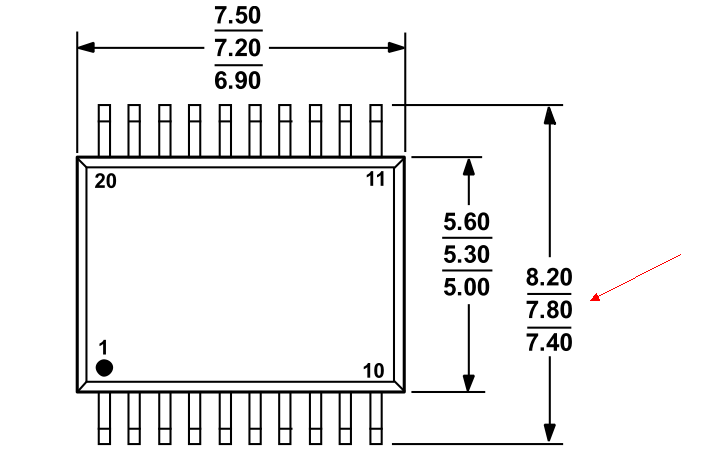
From the data sheet, the width range is easily found to be from 7.40mm to 8.20mm with an
average value of 7.80mm.
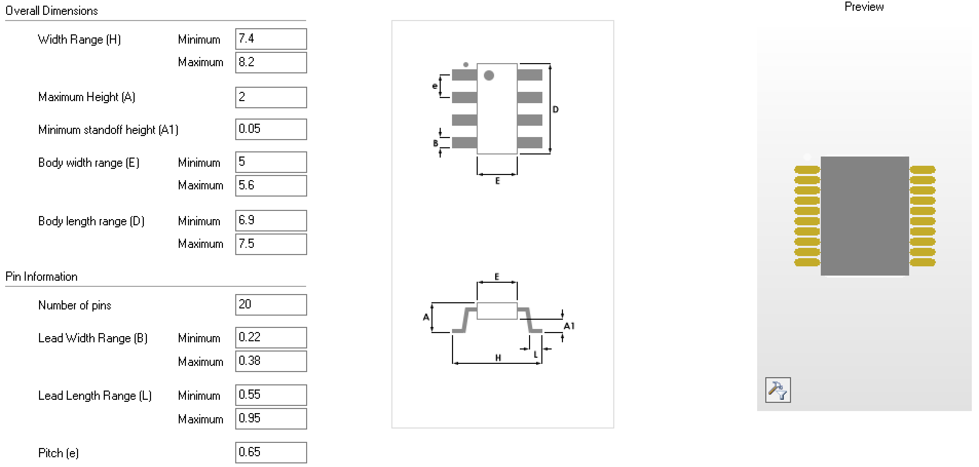
The completed data entry page is attached below for reference:
- Enter thermal pad information if there is. Thermal pad is important for the component to dissipate the excess heat and shall not be ignored!
- Use Altium Designer calculated or default values for the rest of the entries and click next all the way to the last page.

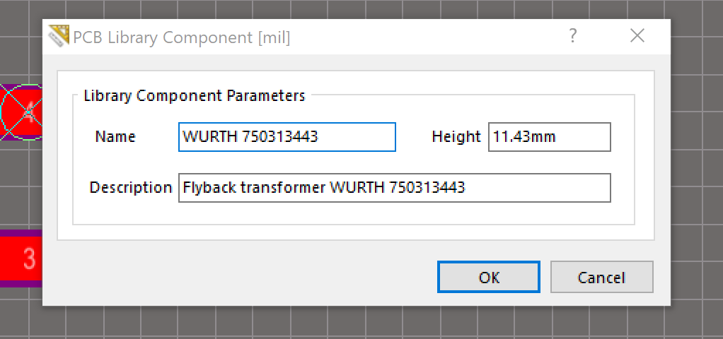
- Change the name and description of the component to appropriate contents. Default name and description are not recommended. Good name and description will help the design in later stages. Your footprint is now completed!
Completely customized footprint
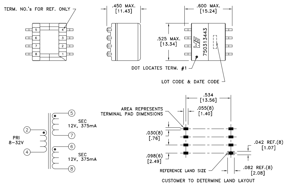
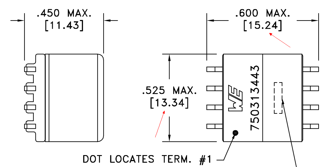
In this example, we will be creating a footprint for ‘WURTH 750313443’, a flyback transformer from Wurth Electronics Midcom. This component is chosen because it is one of the few components I’ve encountered that requires a completely custom drawn footprint. All non-electrical information on the data sheet is attached below.
No matching IPC standard compliant package can be found in IPC Compliant Footprint Wizard for this component. (Although some packages look similar, but you won’t actually be able to fill in the entries). Hence, we are forced to create a footprint from scratch. But keep calm and keep reading, it is not difficult.
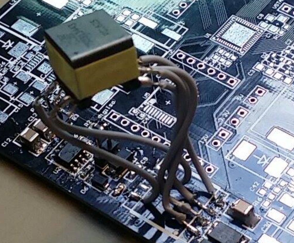
One more thing before we start drawing: The top left diagram in the figure above is a bottom view instead of top view. I unfortunately made a mistake during the first round of prototyping and thought this was a top view. Lucas, my teammate, who did the soldering had to jump wires to make this work. What I meant by jump wires is shown in the photo below, basically it means soldering separate wires to the pads on PCB to reorder the pins. For this component, it is symmetrical and therefore drawing the footprint doesn’t effect anything, only the pin assigning part afterwards was affected.(After the footprint is completed, we have to map the pads to the pins on the schematics diagram)
Now let’s start drawing the footprint!
- Find the useful information from the data sheet and know what they are.
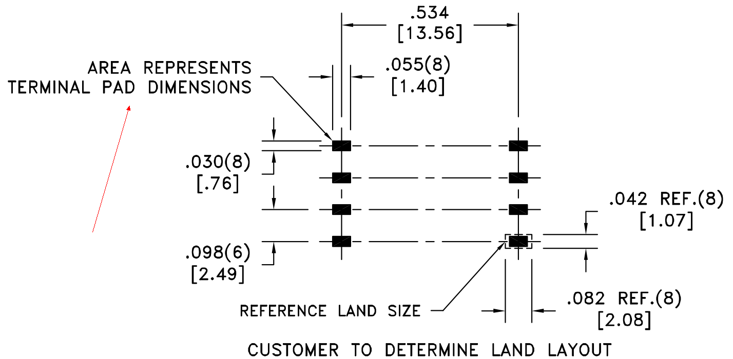
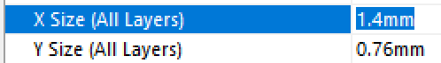
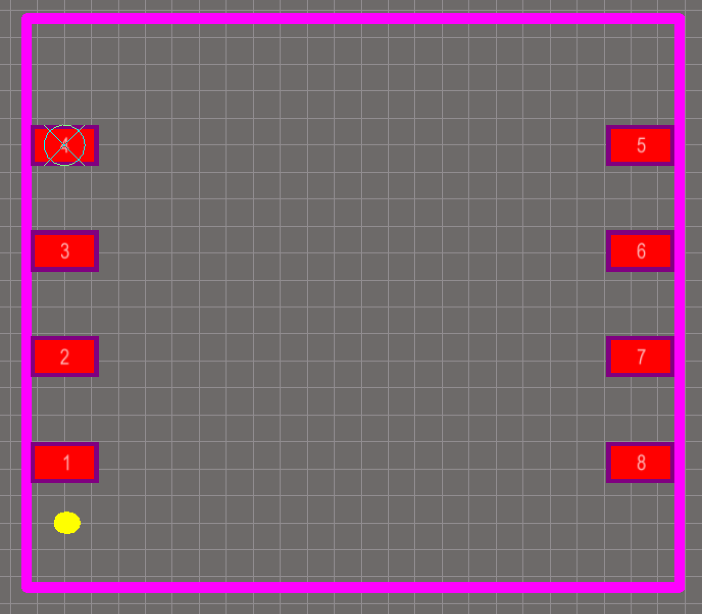
This bottom right diagram gives us all the information we need to draw the pads. ‘Terminal Pad Dimensions’ is what we need to draw the pads, don’t worry about ‘Reference Land Size’. This basically means we need to draw eight identical 0.76mm x 1.40mm size pads. Horizontal intervals between pads are 13.56mm and vertical intervals are 2.49mm.
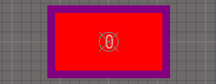
- Draw the first top left pad.
Like using the wizard, we need to first create a PCB library file or open an existing PCB library file. Then click the keyboard twice to place a pad. This pad in its default initial state will be in round shape and for ‘through hole’ type component which has to be changed.
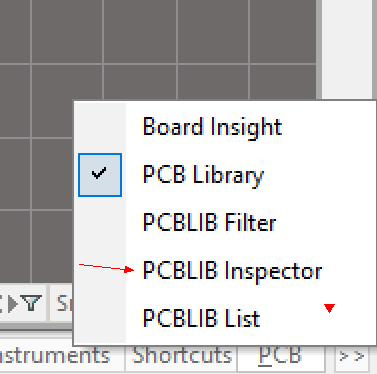
One way to do this is to use the PCBLIB Inspector. This can be opened at the bottom right in Altium Designer.
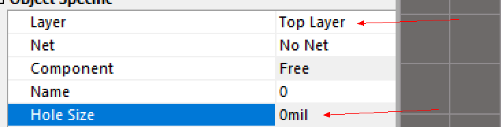
First, we change the shape of the pad to rectangular.

Next, we reduce the hole size to 0 and set the pad to be on top layer instead of multilayer.
Lastly, we set the size of the pad and move it to origin for easier drawing later.
The first pad is now completed:
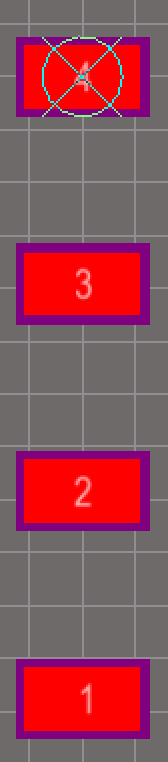
- Draw the rest of the left side pads.
Name the pads according to the data sheet to be ‘4’, ‘3’, ‘2’ and ‘1’.
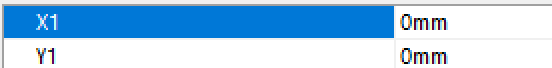
Select all four pads and set their horizontal location to 0mm by changing ‘X1’ in the inspector to 0mm.
Now set the vertical position (‘Y1’ in the PCBLIB inspector) of the pads ‘3’, ‘2’ and ‘1’ to -2.49mm, -4.98mm and -7.47mm.
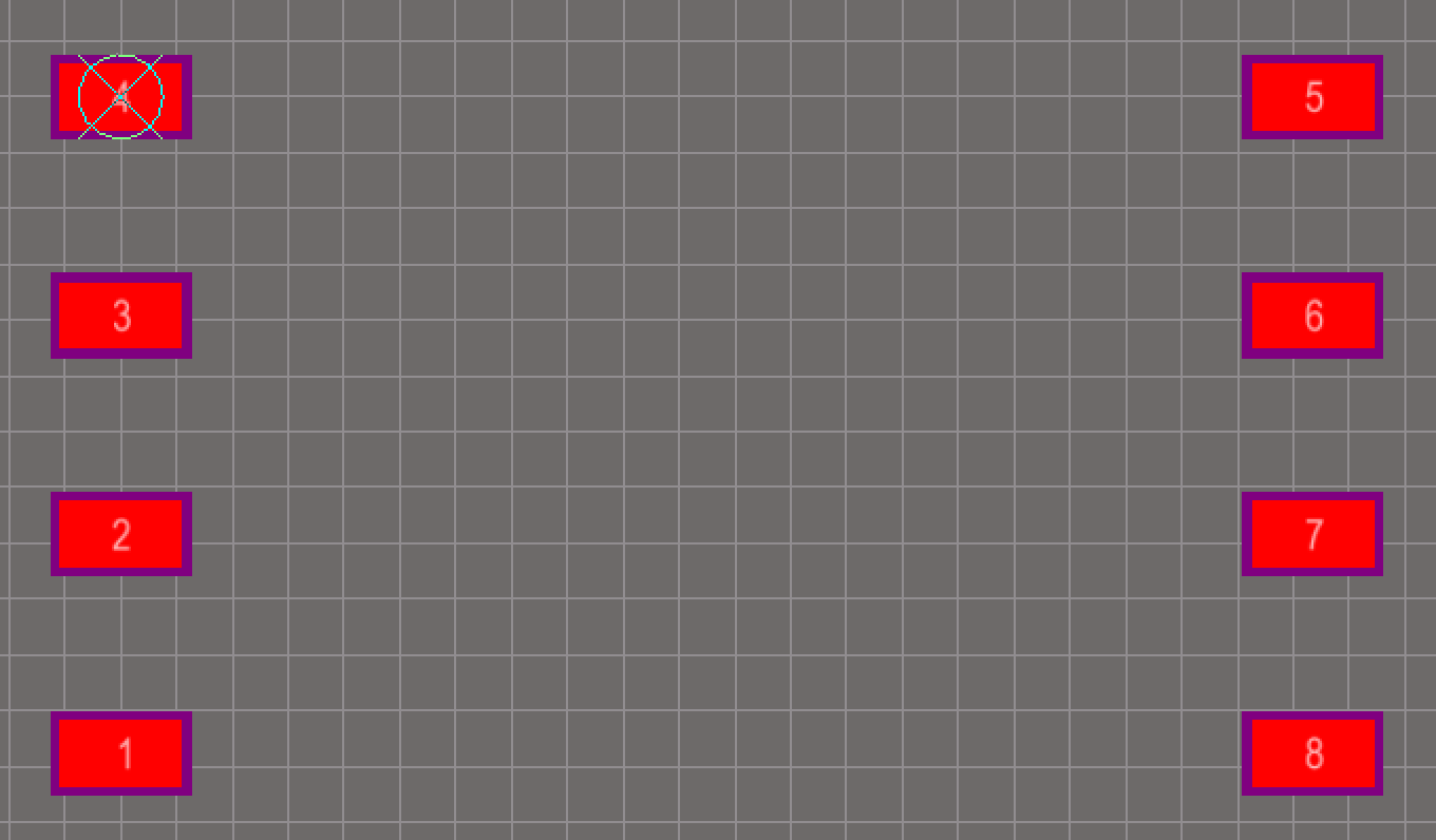
- Draw the right side pads.
Copy all four current pads and paste them somewhere on the right.
Set their names to ‘5’, ‘6’, ‘7’ and ‘8’.
Set their horizontal position to 13.56mm.
Set their vertical position to 0mm, -2.49mm, -4.98mm and -7.47mm if they were not aligned when pasted.
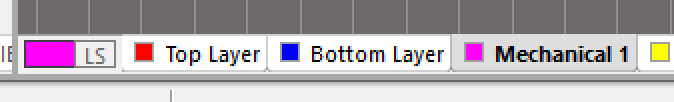
- Draw the mechanical keep-out lines.
We change the current working layer to Mechanical 1 as shown below:
From the data sheet, we know that the transformer is going to need a space of at least 15.24mm x 13.34mm.
Then we simply place lines around the pads which at the same time satisfies the minimum area criteria.
- Place a dot on the layer Top Overlay to note the first pin.
- Open PCB library to change the name and description of the finished component.
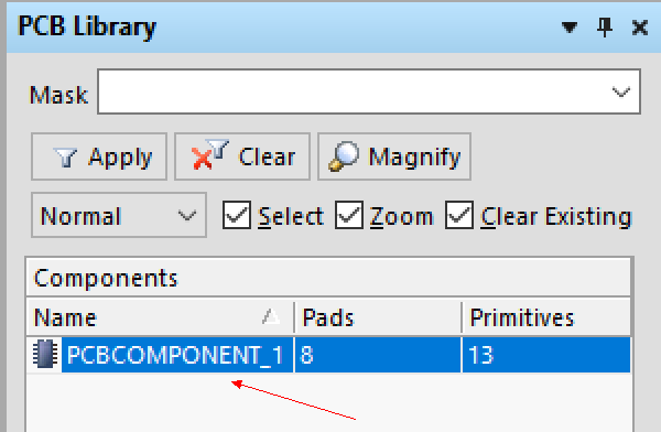
Double click on where it is highlighted and change the name and description to finish the footprint.
TIPs: When making footprints for leadless components (all pins underneath the chip, eg: PQFN), it is always wise to extend the pins outwards for easier hand soldering and debugging purposes.
Congratulations! Now you know how to create a footprint for any component you want and forget the frustration of not being able to find the footprint.
Want to hear more from us? Sign up here and never miss a post! No spam, promise.
About the Author:

Tony Zhang
Lead Battery Systems Management Engineer, 2017